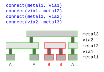
The connectivity setup of a LVS script determines how the connections are made. Connections are usually made through conductive materials such as Aluminium or Copper. The polygons representing such a material form a connection. Connections can be made across multiple polygons - touching polygons form connected islands of conductive material. This "intra-layer" connectivity is implicit: in LVS scripts connections are always made between polygons on the same layer.
Connections often cross layers. A via for example is a hole in the insulator sheet which connects two metal layers. This connection is modelled using a "connect" statement (see connect):
connect(layer1, layer2)
A connect statement will specify an electrical connection when the polygons from layer1 and layer2 overlap. layer1 and layer2 are original or derived layers. "connect" statements should appear in the script before the netlist is required - i.e. before "compare" or any other netlist-related statement inside the LVS script. The order of the connect statements is not relevant. Neigther is the order of the arguments in "connect": connections are always bidirectional.
This is an example for a vertical cross section through a simple 3-metal layer stack with the corresponding "connect" statements:

Labels can be included in the connectivity too. Typically labels are placed on metal layers. If the labels are drawn on the same layer than the metal shapes they are automatically included when using "input" to read the layer. If only labels shall be read from a layer, use "labels" (see labels).
To attach labels to metal layers, simply connect the label and metal layers:
metal1_labels = labels(10, 0)
metal1        = input(11, 0)
via1          = input(12, 0)
metal2_labels = labels(13, 0)
metal2        = input(14, 0)

connect(metal1, metal1_labels)
connect(metal1, via1)
connect(via1, metal2)
connect(metal2, metal2_labels)
If labels are connected to metal layers, their text strings will be used to assign net names to the resulting nets. Ideally, one net is labeled with a single text or with texts with the same text string. In this case, the net name will be non-ambiguous. If multiple labels with different strings are present on a net, the net name will be made from a combination of these names.
KLayout supports implicit connections made across all polygons on a layer, regardless whether they connect or not. A typical case for such a connection is the substrate (aka "bulk"). This connection represents the (lightly conductive) substrate material. There is no polygon representing the wafer. Instead, a layer is defined which makes a global connection with "connect_global" (see connect_global):
connect_global(bulk, "VSS")
The arguments to "connect_global" is the globally connected layer and the name of the global net to create. The function will make all shapes on "bulk" being connected to a single net "VSS". Every circuit will at least have the "VSS" net. In addition, each circuit will be given a pin called "VSS" which propagates this net to parent circuits.
Implicit connections can be useful to supply preliminary connections which are supposed to be created higher up in the hierarchy: Imagine a circuit with a big power net for example. When the layout is made, the power net may not be completely connected yet, because the plan is to connect all parts of this power net later when the cell is integrated. In this situation, the subcircuit cell itself won't be LVS clean, because the power net is a single net schematic-wise, but exist as multiple nets layout-wise. This prevents bottom-up verification - a very useful technique to achieve LVS clean layouts. It also prevents matching in general, as the layout cell will have two pins while the schematic subcircuit has only one. In this case, the cell and subcircuit will never match.
To allow verification of such a cell, "implicit connections" can be made by giving the net parts the same name through labels and assuming these parts are connected: for example to specify implicit connections between all parts of a "VDD" net, place a label "VDD" on each part and include the following statement in the script:
connect_implicit("VDD")"connect_implicit" (see connect_implicit) can be present multiple times to make many of such connections. Implicit connections are accepted on top level, but a warning is issued, indicating that the connection needs to be made further up in the hierarchy. In a subcircuit, implicit connections are required to be connected on the next level of hierarchy - either physically or by another implicit connection. This way, a missing physical connection does not escape and at least a warning is issued if the connection is still not made on top level.
You can declare the layout as being a top level one. This turns the warning about missing physical connections into an error:
top_level(true)
The "connect_implicit" feature is also called "must connect" nets in other systems.
You can include labels of a certain class in a "connect_implicit" statement using glob-style pattern:
connect_implicit("VDD*")This will connect all nets labelled with "VDD1" for example or those labelled with "VDD_5V". However, this statement will only connect "VDD1" with "VDD1", not nets with different labels. I.e. it will not connect "VDD1" with "VDD2" labels. To make connections between differently named nets, use "explicit connections" (see below).
"connect_implicit" can be present multiple times. Each statement extends the choice of labels which will be connected.
The above examples of "connect_implicit" apply to all cells. The statement can be made cell specific, by giving a cell name glob pattern for the first argument, followed by the net name pattern.
The following statement will connect all nets labelled with "VDD" from the "MEMCELL" subcell:
connect_implicit("MEMCELL", "VDD")The rule is applied to all cells matching the glob pattern in the first argument. Again, the "connect_implicit" rule may be given multiple times. In this case, all matching occurrences act together.
The "connect_implicit" statements must be given before the netlist is extracted. Typically this happens before or shortly after "connect" statements.
Explicit connections can be useful to enforce a connection in the layout which is made in the schematic, but not physically on the level of the cell. For example consider the following layout for an inverter:
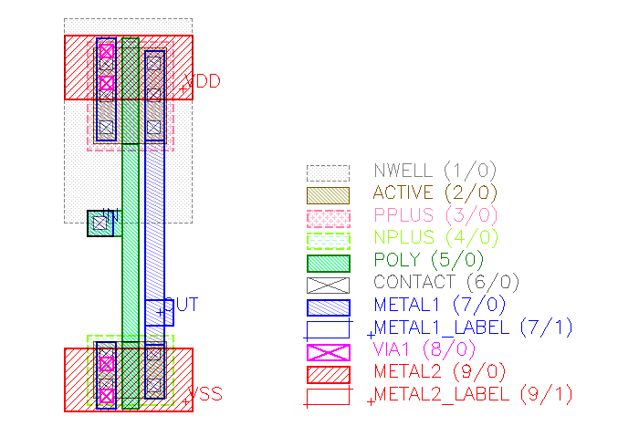
In the layout there are no tie-down diodes, hence there is no physical connection to the n-well region and no physical connection to the bulk substrate. This saves space, but these diodes need to be added by other ways. Usually this is done when the standard cells are combined into macros. Filler cells will be added which include these substrate and well contacts.
On the inverter level however, there is no such connection. Therefore the inverter has separate bulk and n-well pins. The schematic sometimes is a simplified version which does not offer these pins. Hence there is an intrinsic mismatch between layout and schematic.
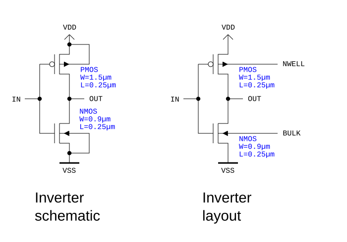
To align layout and schematic, bulk and VSS pins can be connected explicitly. Same for n-well and VDD. This scheme is similar to the "connect_implicit" scheme explained above, but can connect differently named nets.
To establish an explicit connection in the above example, make sure that n-well and bulk have proper names. For the n-well this can be done by creating labels on the n-well islands giving them a proper name - e.g. "NWELL". The bulk isn't a real layout layer with polygons on it. Using "connect_global" will both connect everything on this layer and give it a name.
The following code will connect the bulk net with "VSS" inside the cell "INV":
connect_global(bulk, "BULK")
...
connect_explicit("INV", [ "BULK", "VSS" ])
Note that this rule will form a new net called "BULK,VSS" combining both subnets.
The cell name can be a pattern. For example "INV*" will apply this rule on all cells starting with "INV". The cell pattern is not mandatory: if it is omitted, the rule is applied to all cells.
Like implicit connections, explicit connections are checked for being made on the next level of hierarchy, either physically or by another explicit or implicit connection.
An explicit connection will also imply implicit connections on the nets listed in the net names. So in the example above, different pieces of "VSS" are connected even if they are not physically connected. Again, it is checked that these connections are made later up in the hierarchy.
Again, the "connect_explicit" statements must be given before the netlist is extracted. Typically this happens before or shortly after "connect" statements.
Soft connections are a way to find wiring issues where signals or even power is routed over high-ohmic paths. High-ohmic paths can be established through connections via poly silicon, implant, well or substrate areas. Such areas can easily show resistance values which are a hundred times higher than that of metal connections. We have to make sure that for routing power or critical signals, connections are not made through such areas, but primarily through metal connections.
Here is an example:
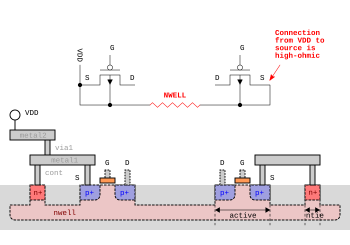
In this case, we have a standard textbook planar CMOS technology with two PMOS devices sitting in a n-well. These could be the two PMOS of two inverter pairs for example. Both PMOS need to be connected to VDD at their sources. In addition, the n-well area also needs to be tied to VDD in order to provide reverse bias for the p+ drain areas and the body potential for the transistors, forming the opposite electrode of the gate capacity.
Such a technology stack can be described by the following connectivity:
# Input layers

nwell = ...
active = ...
pplus = ...
nplus = ...
poly = ...
contact = ...
metal1 = ...
via1 = ...
metal2 = ...

# computed layers

(nactive, pactive) = active.and_not(nwell)

# PMOS and NMOS source/drain regions
psd  = (nactive & pplus) - poly
nsd  = (pactive & nplus) - poly

# n tie and p tie (nwell and substrate contact)
ntie = nactive & nplus
ptie = pactive & pplus

# connections

# nwell connections
connect(ntie, nwell)
connect(contact, ntie)

# substrate connections
connect_global(ptie, "BULK")
connect(contact, ptie)

# device connections
connect(contact, psd)
connect(contact, nsd)
connect(contact, poly)

# metal connections
connect(metal1, contact)
connect(via1, metal1)
connect(metal2, via1)
However, there is an issue: As shown in the picture, the left PMOS source is properly connected to VDD. The right one however lacks the metal connection to VDD. From the perspective of pure connectivity, this transistor's source is connected to VDD, but only through a weak n-well connection. Such a device will not work - or at least, badly.
The solution is to introduce soft connections. Soft connections are made by replacing "connect" with "soft_connect" and "connect_global" with "soft_connect_global" (see soft_connect and soft_connect_global). The first layer is the "upper" layer while the second layer is the "lower" layer. The lower layer is the high-ohmic one. In global connections, the global net is always the high-ohmic one.
Soft connections can be visualized as directional connections: current can only flow from the upper to the lower layer, but not the other way. So, a real connection is only made, if both upper terminals of the soft connections are connected to the same physical net.
To solve the n-well issue we have to substitute the n-tie to n-well connection statement by a "soft_connect" statement:
soft_connect(ntie, nwell)
The above picture now looks like this:
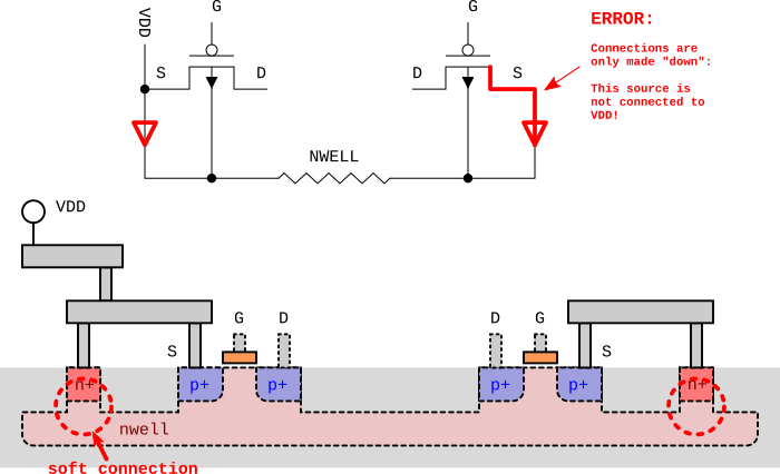
With this definition, the netlist extractor is able to detect the fault and raise a warning or an error (in top level mode). The warning is shown on the log tab and indicates incomplete wiring plus details about the subnets, separated by the soft connections.
The complete the setup we also need to include other soft connections, such as connections via substrate (a global soft connect to the BULK net), via source/drain implants, via the tie implants and via poly:
# Input layers

nwell = ...
active = ...
pplus = ...
nplus = ...
poly = ...
contact = ...
metal1 = ...
via1 = ...
metal2 = ...

# computed layers

(nactive, pactive) = active.and_not(nwell)

# PMOS and NMOS source/drain regions
psd  = (nactive & pplus) - poly
nsd  = (pactive & nplus) - poly

# n tie and p tie (nwell and substrate contact)
ntie = nactive & nplus
ptie = pactive & pplus

# connections

# nwell connections
soft_connect(ntie, nwell)
soft_connect(contact, ntie)

# substrate connections
soft_connect_global(ptie, "BULK")
soft_connect(contact, ptie)

# device connections
soft_connect(contact, psd)
soft_connect(contact, nsd)
soft_connect(contact, poly)

# metal connections
connect(metal1, contact)
connect(via1, metal1)
connect(metal2, via1)
As this code demonstrates, multiple soft connections can be specified. From the perspective of the check, all soft connections are of the same kind.
Note, that two opposite soft connections cancel, so this would eventually make a hard connection:
soft_connect(a, b)
soft_connect(b, a)
NOTE: It is therefore important to observe the direction of soft connections: upper and high-conductive / low-ohmic layer first, and lower and low-conductive / high-ohmic layer second.
Soft connections and must connect nets (aka "connect_explicit" and "connect_implicit") serve the same purpose - to detect incomplete wiring. Typically they are used together, such as doing "connect_implicit" on VDD nets and "connect_explicit" on VDD and NWELL nets if the schematic circuits do not feature an explicit NWELL pin.
Soft connections are checked before connect_explicit and connect_implicit are executed. This means, that soft connection errors cannot be masked by declaring them "must connect". On the other hand, that is not a real issue as both checks would raise an warning or error (in the top-level case). It would only be a different kind of warning.